Circuit Design
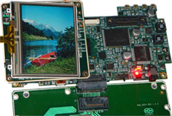
The EnCADIS Design team has the experience and expertise to cost effectively develop designs that meet your product requirements and address your time to market. We understand that a high quality and manufacturable circuit design is a critical step in the implementation of electronic products. Our proven methodology and design process ensures design quality and minimizes development time. Our extensive experience designing a portfolio of successful products maximizes your probability of a working design that is manufacturable and reliable. EnCADIS Design's methodology and process are specifically aimed at minimizing overall development schedules and cost, while ensuring production ready, first time working designs.
Design Capabilities
- Circuit Boards
- Backplanes
- High-Speed/High-Density Designs (30 Layers)
- Signal Integrity Simulations (HyperLynx, Spectra, HSpice)
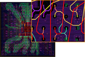
- Layout and Routing (Cadence, Mentor, OrCAD)
- Timing and Synchronization
- Processor/Memory Sub-Systems (i.MX, OMAP3, XScale, DDR2, DDR3, QDDR)
- Modular Reusable Sub-Designs
- Handheld Units - Battery Powered (Li-Ion, NI-MH)
- RF Design (Wi-Fi, Wireless USB, ZigBee, Bluetooth)
- Fault Tolerant Systems
- Power Supply Design (Charging, Boost, Buck, LDO)
- Hot Plug-In and Power Sequencing
- Power Management and Fuel Gauges
- Thermal Management
- PCB Stack-Up Design and Optimization
- Controlled Impedance Routing (Successful Design to 10 Gb/s)
- Blind and Buried Via Design
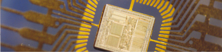
- ASIC Substrate Design
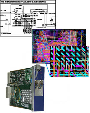
Schematics - Layout/Routing - Prototype Build
EnCADIS Design team's reputation is built on a long standing record of building working and manufacturable designs on the first iteration. Whether the design entails a high speed XFP based 10Gb/s interface, a dense high-speed 24 layer ADM Switch Fabric, or a small 8 layer wireless consumer product, the ability to take the design from schematics to prototype build, allows us to manage the entire design flow and optimize appropriately at each step. Our proven design process incorporates DFM guidelines to ensure that the designs are manufacturable with high yields by Tier 1, Tier 2, and quality Tier 3 CMs. At EnCADIS we'll manage the entire process through delivery of fully tested prototypes and manufacturing introduction and ramp. Component procurement is tightly coupled with the design process to ensure all materials are available for prototype build.
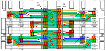
Backplane Technology
EnCADIS' backplane development process and design techniques ensure backplane routing optimization and high signal integrity. Our portfolio of completed backplanes includes a 26 layers 2 Terabits per second design supporting hot plug-in, redundant power, and 3.125 Gb/s differential pair signaling (characterized to run over 6 Gb/s). We have experience and expertise with both Rogers and Nelco materials, high speed interconnect systems, and proprietary technology for minimizing EMI, crosstalk, and other radiation effects on high-speed backplanes.
Substrate Design and Routing
EnCADIS provides ASIC substrate design and routing for high-speed ASICs. Our designs have included differential controlled impedance routing, proprietary techniques for cross-talk reduction, and optimally placed power supply filtering. We have worked with substrate suppliers such as Kyocera, to deliver first iteration working substrates with a large number of signals running at 1.25 Gb/s (LVDS) and 3.125 Gb/s (CML) for ASICs with over 1500 pins/balls.